Imina Technologies’ modular robotic platforms are designed to fit all kind of scanning electron microscopes and optical setups. Probing at MICRO and NANO scales becomes truly convenient.
Imina Technologies’ modular robotic platforms are designed to fit all kind of scanning electron microscopes and optical setups. Probing at MICRO and NANO scales becomes truly convenient.
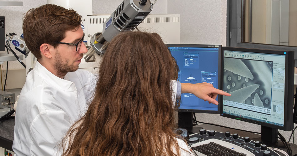
Bring probe tips in contact with semiconductor chips, measure the electrical characteristics of integrated components, localize defects and isolate structures, in your SEMs, FIBs and Dual Beams.
Precisely position probes and sensors under your optical microscopes, probe stations and inspection tools. And physically interact with your samples in even the most confined environments.
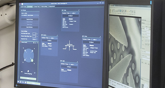
Make your electrical probing journey intuitive and efficient with Precisio™, a unified Software Suite, allowing you to control your setup within the full testing process.
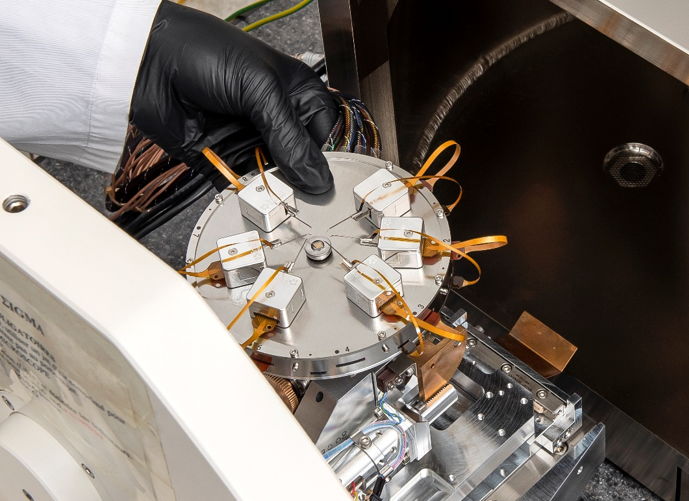
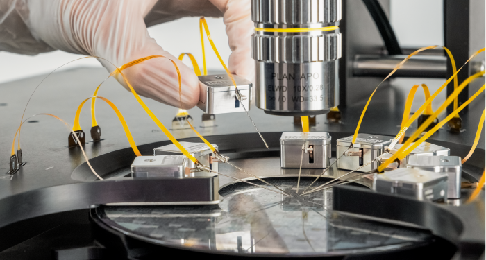
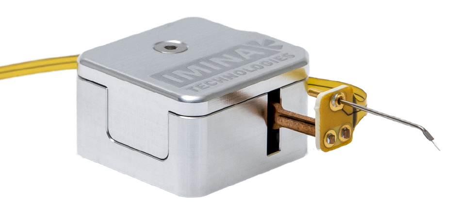
A unique mobile piezo motion in a compact robot.
Imina Technologies’ core technology resides in the unique integration of piezoelectric actuators into the miBot™, the world’s most compact 4 degrees of freedom robot with nanometer resolution of positioning. Contrary to traditional manipulators, the miBot is a mobile robot. It is virtually untethered and free to move over the surface of its stage. Since it has no mounting screws, the miBot can be coarsely positioned by hand in arbitrary positions and naturally adapts to changing samples geometries and microscope configurations.
Sub-nm resolution over cm traveling ranges |
✓ |
Combination of coarse and fast movements over centimeter distances and fine sub-nanometer movements.
|
Unmatched flexibility |
✓ |
Flexible installation for straight forward adaptation to different experimental setups and specimens. |
High stability |
✓ |
High mechanical and thermal stability guarantees stable positioning over long periods of time, from 0° up to 55° tilt angle. |
Short learning curve |
✓ |
Easy to control for reduced risk of sample and probe damage and fast access to measurements. |
Compatible with any microscope |
✓ |
Compatible with high resolution imaging using magnetic lenses to contact samples under low accelerating voltages and short working distances. |
Vertical fine-motion range up to 15 µm |
✓ |
Easy, rapid and safe probe-landing for few-nm technology nodes or other samples that require low-kV and short working distance imaging conditions. |
We used Imina Technologies’ nanoprobing service to investigate a yield issue in 12 nm CMOS with 30 nm VIA0 probe pads. First we discussed the tasks, sample preparation, layout, and locations for probing. Then we used Imina’s state-of-the-art nanoprobing solution to navigate the delayered sample and to measure the IV curves on many different transistors, without damaging a single probe pad, and all in one day.s
Full documentation was provided the same day. And most importantly, my customer was happy with the results.

Dr. Piet De Pauw
IMEC
Using miBots in our FIB system, I was able to rapidly probe individual semiconductor nanowires with sharp, FIB-milled probes. Being able to do this quickly enough to probe a large (~150) number of wires was crucial for the study, as it enabled a statistical approach to the characterization. This would have been impossible without easy access to a flexible and precise nanoprobing solution like the miBots.

Alexander Bosberg
SuperSTEM Laboratory
Recently, I have set up the in situ/operando SEM using Imina Technologies SA nanoprobes to observe the morphology and structure changes in various battery materials during the charging/discharging process. These nanoprobers can be combined with different setups to provide valuable insights about materials. As I support many researchers, I handle a wide variety of samples for different applications, which come in different shapes and sizes. Imina tools and their software are very intuitive, the probing is easy, and I feel very confident as a user.
Dr. Kim
KIST
When the miBots and nanoindenter are used together, electrical characterization can be done while localized mechanical stress up to GPa-level is applied to the device. This approach opens up a new chapter on the combined mechanical stress and electrical measurements.

Kookjin Lee
KU Leuven and imec
The miBots help accelerating tests of our micro-chips by allowing us to make direct electrical contacts with the circuits, avoiding the time-consuming wire-bonding process. Thanks to their freedom of motion, we can easily change their orientation and approach the probe to the sample with always the most appropriate angle. This unique capability is really useful for us when it comes to take out breakable frames from our MEMS.

Dr. Klaus Schimmanz
BTU Cottbus-Senftenberg
miBots are an invaluable tool for nanoscience research in our group. We rely on them for making electrical contacts to various optoelectronic samples.

Joeson Wong
Atwater Research Group in Caltech
The most remarkable property of Imina system is its scalable positioning which enables both centimeter- and nanometer-range positioning travel range. I can approach different destinations on my sample to contact my nanoparticle structures. Imina’s nanoprobers are flexible, easy, fast to use, and I can see everything I do with the structures in real time.

Stefan M. Schupp
University of Konstanz
The mobile robots from Imina Technologies are the piece of technology that is missing to the family of AFM-based techniques. They combine key requirements for the in-line monitoring and diagnostic instruments that we are jointly developing in the EU Project NANOHEAT that will allow wafer-level interoperation control.

Dr. Wladek Grabinski
EPFL, Nanoelectronic Devices Laboratory
The compact design of the platform makes the installation in our SEM really convenient and fast. This avoids cluttering the microscope with accessories used for the manipulation and probing of nanowires when other measurements are made.

Dr. Nicolas Blanchard
UCBL1, Institute of Light and Matter
We needed a tool to precisely position our semiconductor ZnO nanowires under our optical instruments, and we were really amazed to see how fast we were able to get results with the miBot micromanipulators.

Dr. Christophe Couteau
UTT, Laboratory of Nanotechnology
We are using the miBots for micro-assembly of diamond structures glued on larger silicon cantilever. Their flexibility and easiness of use make them particularly suitable for such applications where dexterity is essential. Moreover, they can be quickly installed and removed from a microscope, allowing us to always operate in the best conditions adapted to the diamond size.

Dr. Claudia Widmann
Fraunhofer IAF
My students love it! The miBot is so easy to use that it only takes them a few minutes to learn before they can actually start making the electrical measurements of their lab assignment.

Dr. Rosendo Sanjines
EPFL, Institute of Condensed Matter Physics
We use miBots to probe the electrical properties of Si microwires that we grow. They have been invaluable for measuring I-V curves and the contact resistance of Ni nanoparticles deposited on the wires. The fine motion and stability of the miBots along with the intuitive interface made these measurements quick and easy to perform.

Dr. Dan Turner-Evans
Caltech, Applied Physics, Atwater Group
Because it's very intuitive to move a probe over several millimeters and position it with nanometer resolution on the target, we can now load several devices to test side by side in the SEM and process them successively, without having to open the chamber between two. Besides this, the compactness of the miBots and its low dissipation power result in extremely small temperature drifts at the probe tips and, as a direct consequence, to very stable electrical measurements.

Jörg Jatzkowski
Fraunhofer IMWS
Time is critical for us: the more data we collect, the better is the characterization of our nanostructures. Imina Technologies micromanipulators help go in that direction by drastically reducing the time we spend per experiment.

Prof. Anna Fontcuberta i Morral
EPFL, Laboratory of Semiconductor Materials
We have a fully equipped demo lab for semiconductor electrical failure analysis. Our applications team is eager to perform live demonstrations and feasibility studies for you, onsite or online.
In the meantime, do not miss the opportunity to learn more about our products and applications with one of our webinars!