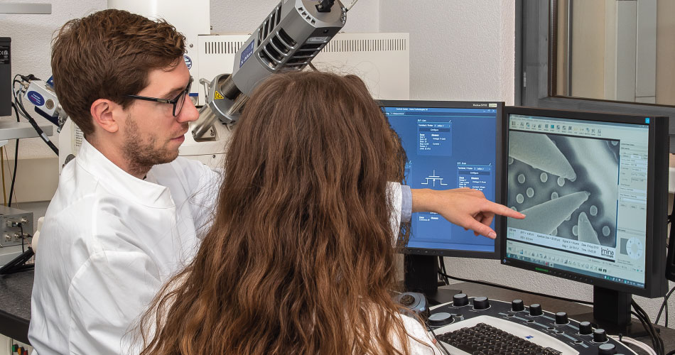
With the continuous shrinkage of the component size of integrated circuits (IC), nanoprobing in scanning electron microscope (SEM) has become an increasingly used technique by IC design and failure analysis engineers to characterize the performance of microchips, as well as to locate and analyze the root cause of defects.
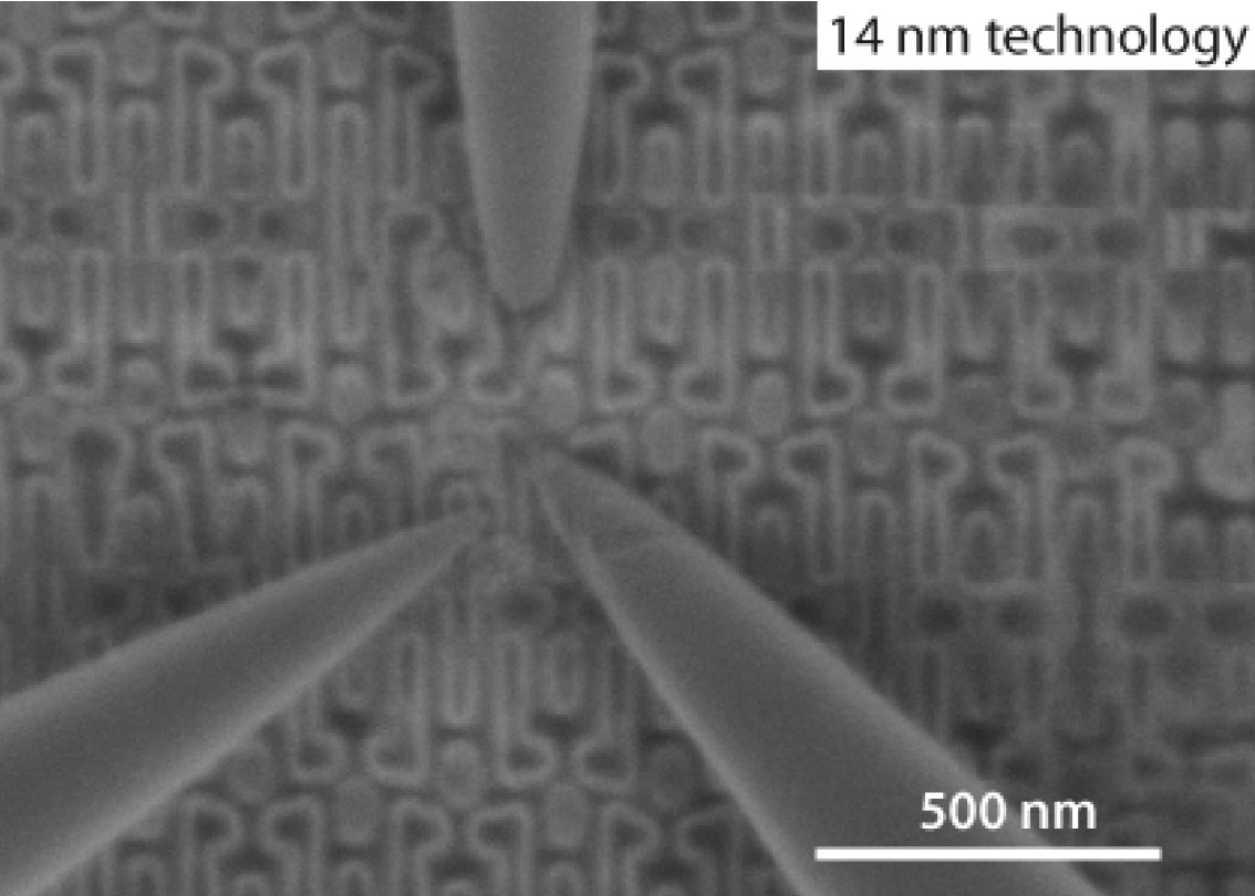
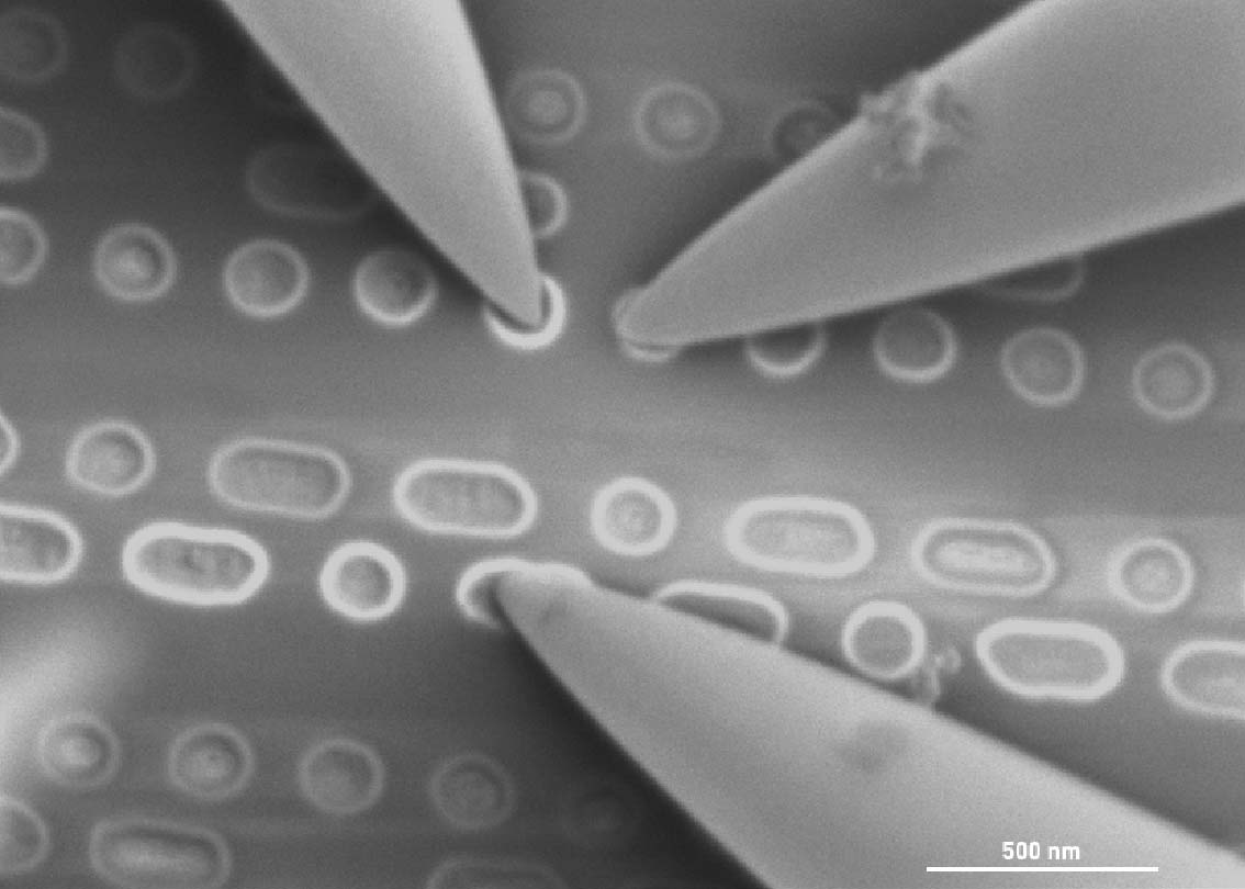
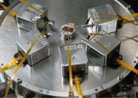
In this note, we report an application of Imina Technologies’ Nanoprobing Solution to characterize NMOS and PMOS transistors of commercially available processors of 22 nm, 14 nm, and 10 nm technology nodes. Measurements on the 10 nm device are reported and discussed. The experiments were carried out at different sites in two different SEM with no permanent modifications required of the microscopes.
The results showed that the unique motion technology of the miBot™ nanoprobers helped to position probe tips with ease on the device under test. Their compact design proved to be advantageous to maintain stable electrical contacts for over 10 minutes to more than an hour.
Precisio™ software was used throughout the entire process, from positioning the probes and landing them in with the transistor nodes, to the configuration of test recipes and acquisition of measurements by remotely controlling the semiconductor parameter analyzer.
We have fully equipped demo lab for semiconductor electrical failure analysis. Our applications team is eager to perform live demonstrations and feasibility studies for you, onsite or online.
In the meantime, do not miss the opportunity to learn more about our products and applications with one of our webinars!