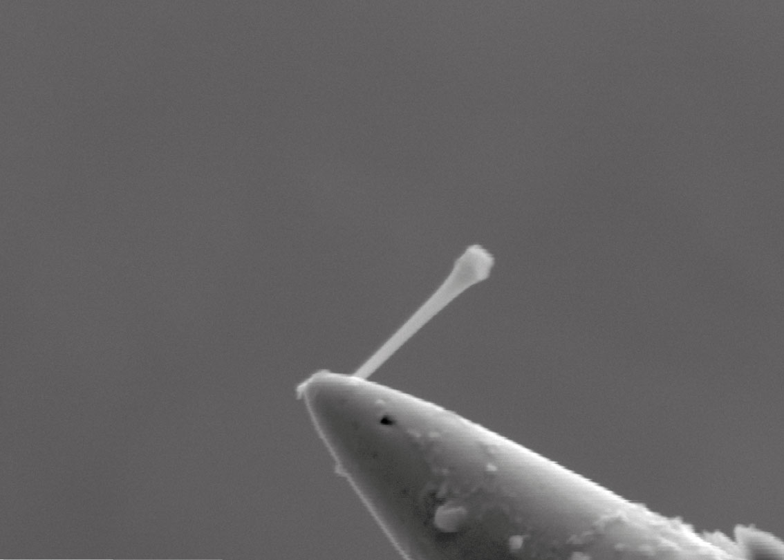
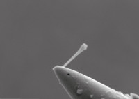
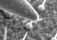
Nanoscale objects, such as nanowires and nanoparticles, can't be seen under the optical microscope due to the diffraction limit. So they have to be observed in a scanning electron microscope (SEM). Inside SEM, under vacuum conditions, forces experienced by nanoscale objects are different from those at macroscale: the gravity is negligible, while van der Waals, or weak electrostatic, forces dominate.
This application note offers the reader an understanding of the forces acting on objects at nanoscale, and a few tips and tricks to manipulate such objects in the SEM more efficiently.
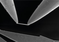
The experimental section shows how to pick up nanowires from a native substrate and transfer them to another substrate.
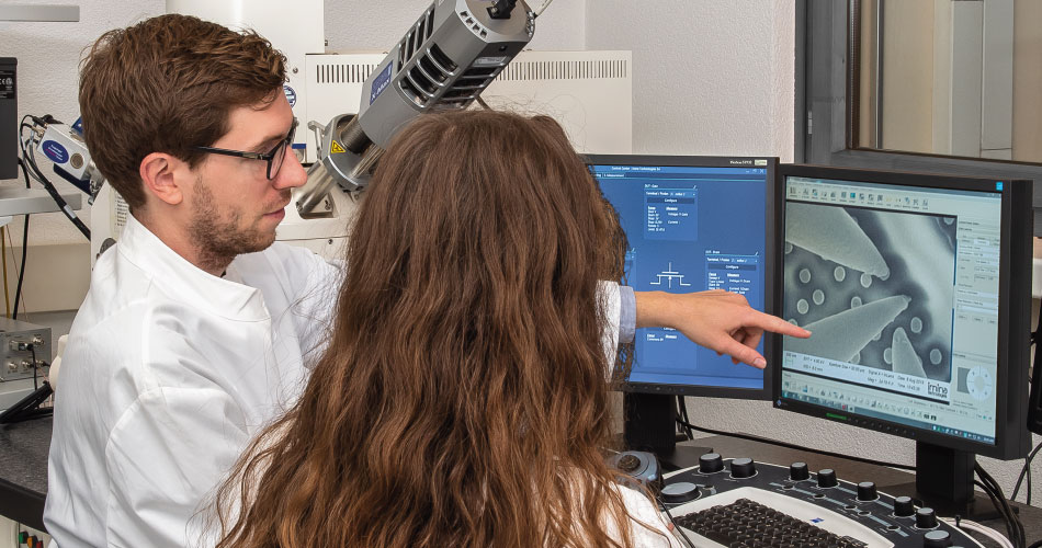
The experiment is carried out in a MERLIN SEM from Carl Zeiss with the Nanoprobing SEM Solution from Imina Technologies equipped with 4 miBot™ nanomanipulators.
National Enterprise for nanoScience and nanoTechnology (NEST), Pisa, Italy
We have fully equipped demo lab for semiconductor electrical failure analysis. Our applications team is eager to perform live demonstrations and feasibility studies for you, onsite or online.
In the meantime, do not miss the opportunity to learn more about our products and applications with one of our webinars!