Piezoelectric nanowires are actively researched as they can serve to create microsensors with high sensitivity resolution for force and pressure sensing.
This application note shows how to characterize the electrical response from bending individual GaN nanowires.
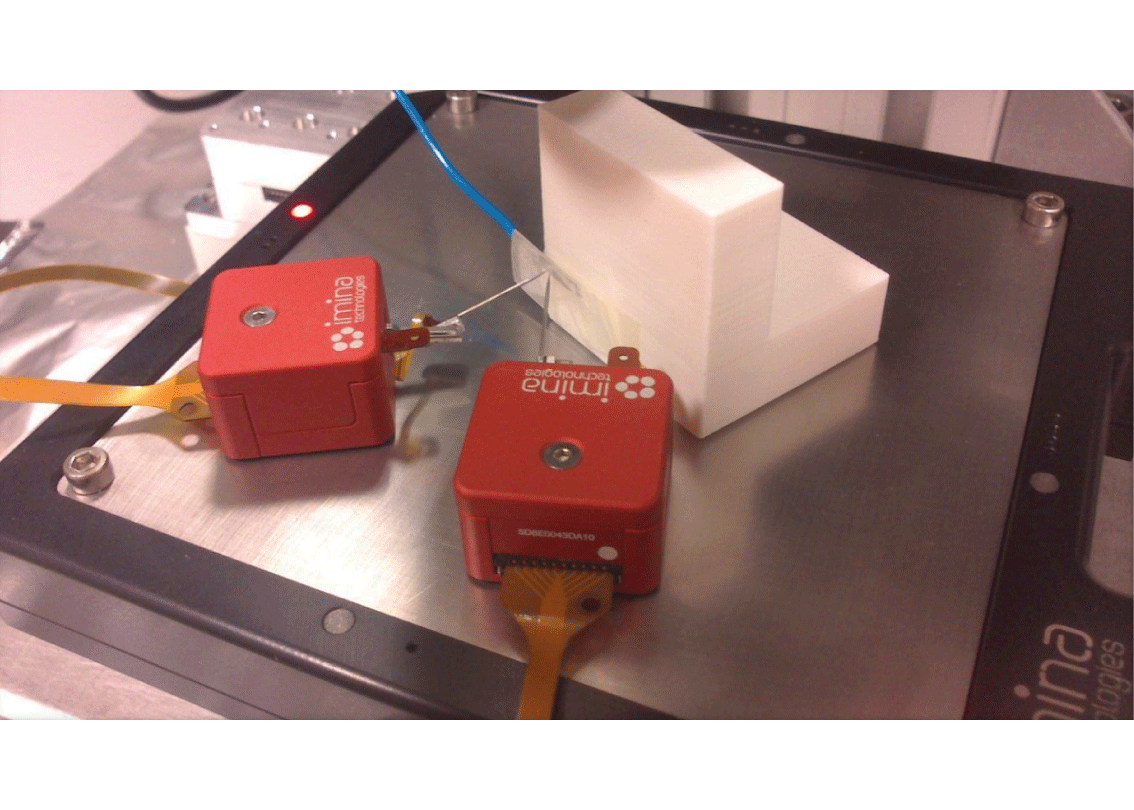
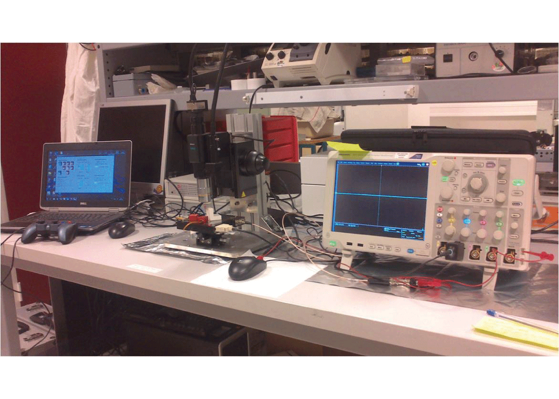
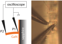
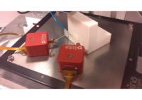
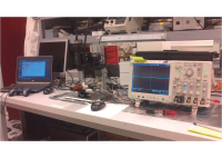
This experiment features two electrical probes mounted on miBot nanomanipulators and connected to an oscilloscope (Agilent Technologies) via a voltage amplifier with high input impedance.
The probes were used to contact each nanowire at the base and at the top. The top probe pressed the nanowire in order to bend it.
The oscilloscope was parameterized in differential mode measured the difference of potential between the probe tips, representing the piezoelectric response of the bended nanowire. Response peaks around 30mV were measured for nanowire bent of ca. 3um.
MiBot micro-robots on a portable platform were easy to integrate under a light microscope. Thanks to the robots' intuitive motion control in 4 degrees of freedom, it was quick and easy to contact the micron-scale structures.
The mechanical characteristics of a nanowire can be determined by modeling it as beam with a fixed end. Young's modulus can be calculated by bending the nanowire with a rigid probe and using the image from the microscope (SEM or optical) to measure the deflection.
Emmanuelle Pauliac-Vaujour, Sven Salomon, Joël Eymery, Edgar Leon Perez. Self-Powered Conformable Deformation Sensor Exploiting the Collective Piezoelectric Effect of Self-Organised GaN Nanowires, Le Cam, Vincent and Mevel, Laurent and Schoefs, Franck. EWSHM - 7th European Workshop on Structural Health Monitoring, Jul 2014, Nantes, France. 2014.
We have fully equipped demo lab for semiconductor electrical failure analysis. Our applications team is eager to perform live demonstrations and feasibility studies for you, onsite or online.
In the meantime, do not miss the opportunity to learn more about our products and applications with one of our webinars!