In this application note, we show how to locally characterize the electrical response of solar cells and photovoltaic (PV) materials using Imina Technologies' miBot micromanipulators
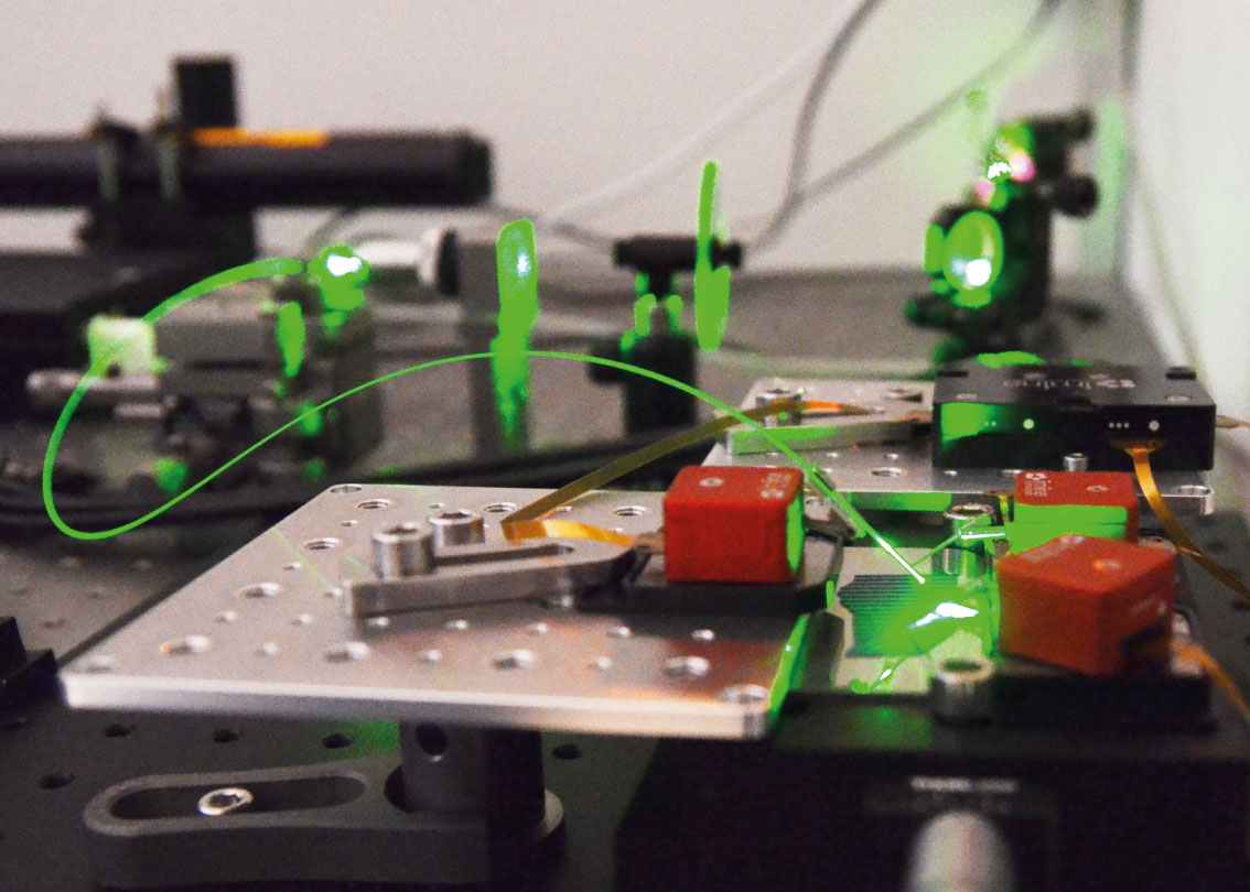
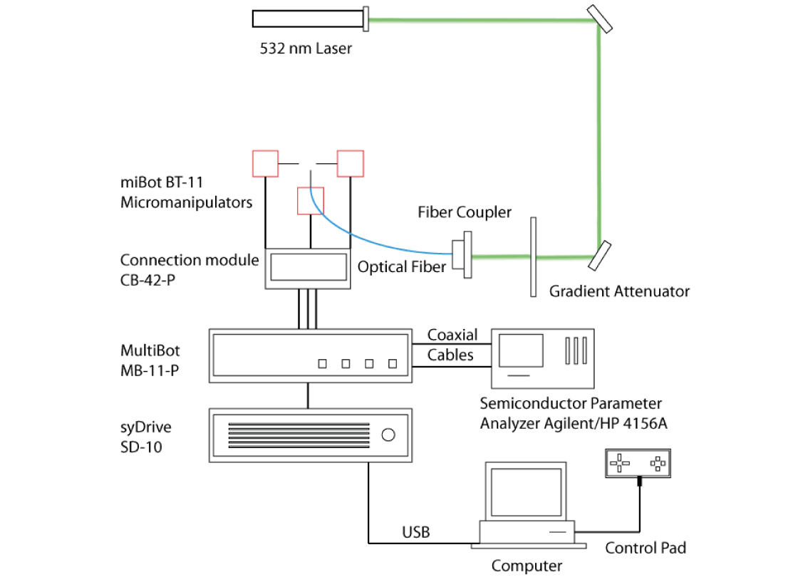
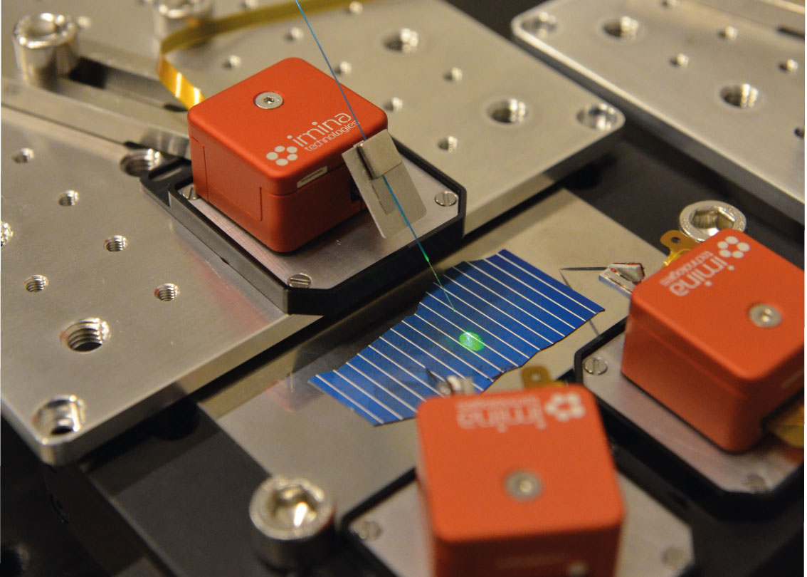
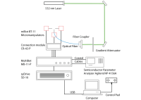
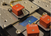
We describe the setup that uses one miBots to precisely position and control an optical fiber coupled with a laser source above the sample surface, and another two miBots to electrically contact the device.
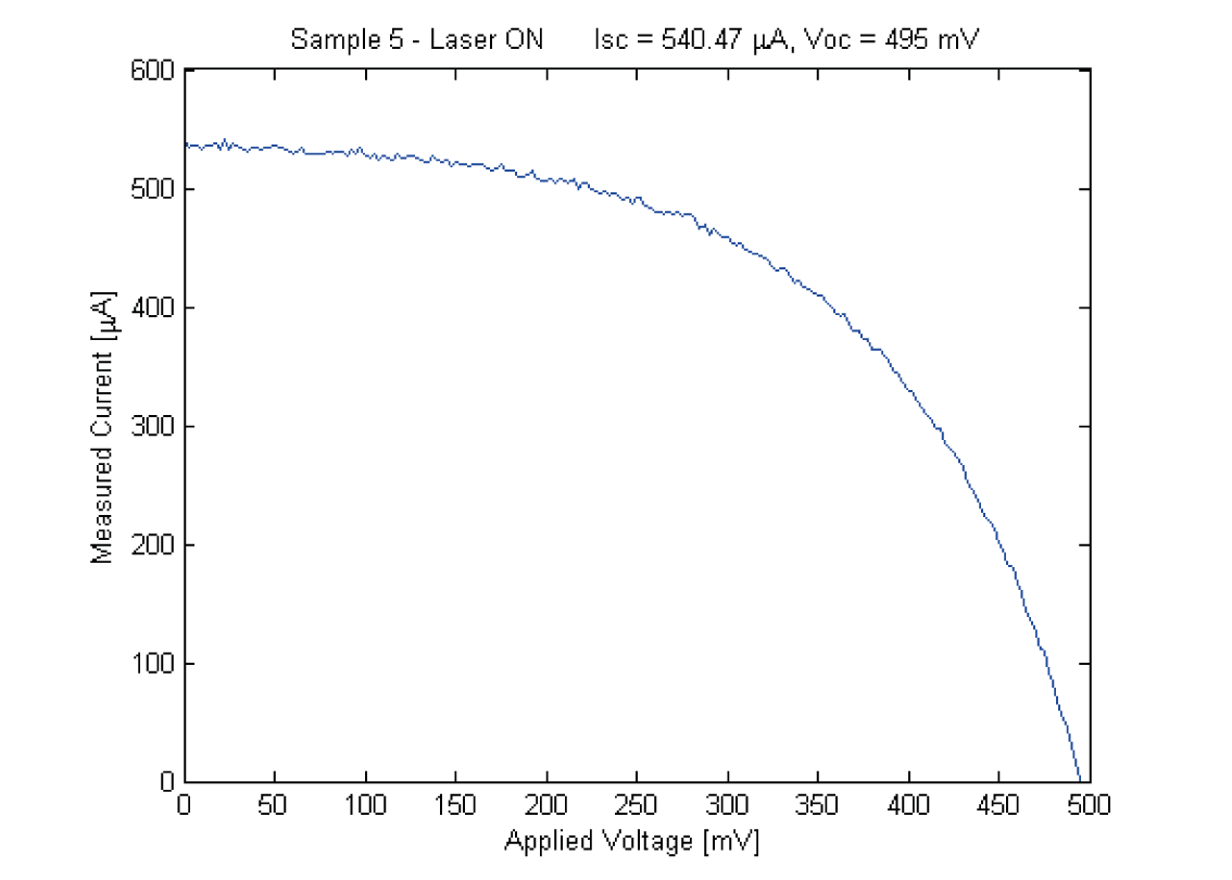
First, we determine the current-voltage characteristics of the samples using a forward bias under illuminated conditions, using an Agilent/HP 4156A semiconductor parameter analyzer.
Then we examine the uniformity of the PV devices by measuring the current while the laser spot is moved along the sample in a line.
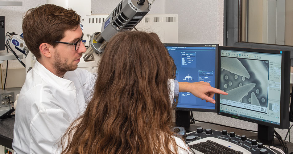
We have fully equipped demo lab for semiconductor electrical failure analysis. Our applications team is eager to perform live demonstrations and feasibility studies for you, onsite or online.
In the meantime, do not miss the opportunity to learn more about our products and applications with one of our webinars!